Jürgen
PCB Specs: During this week i started working on the schematic and PCB design for the sensor matrix. On our meeting on Wednesday we decided on a minimum and desired scanning frequency for the whole matrix / half matrix (one board). To achieve a minimum scan rate of 40 Hz on 88 Sensors, in average evaluating one LDR-sensor must not take more than 0.28 ms, equals to a sampling freq. of 3520 Hz. To achieve the desired 100 Hz, a analog sampling frequency of 8800 Hz is required, which would be close to the limit of approx. 9500 Hz (without overclocking the ADC) of the Arduino Nano.
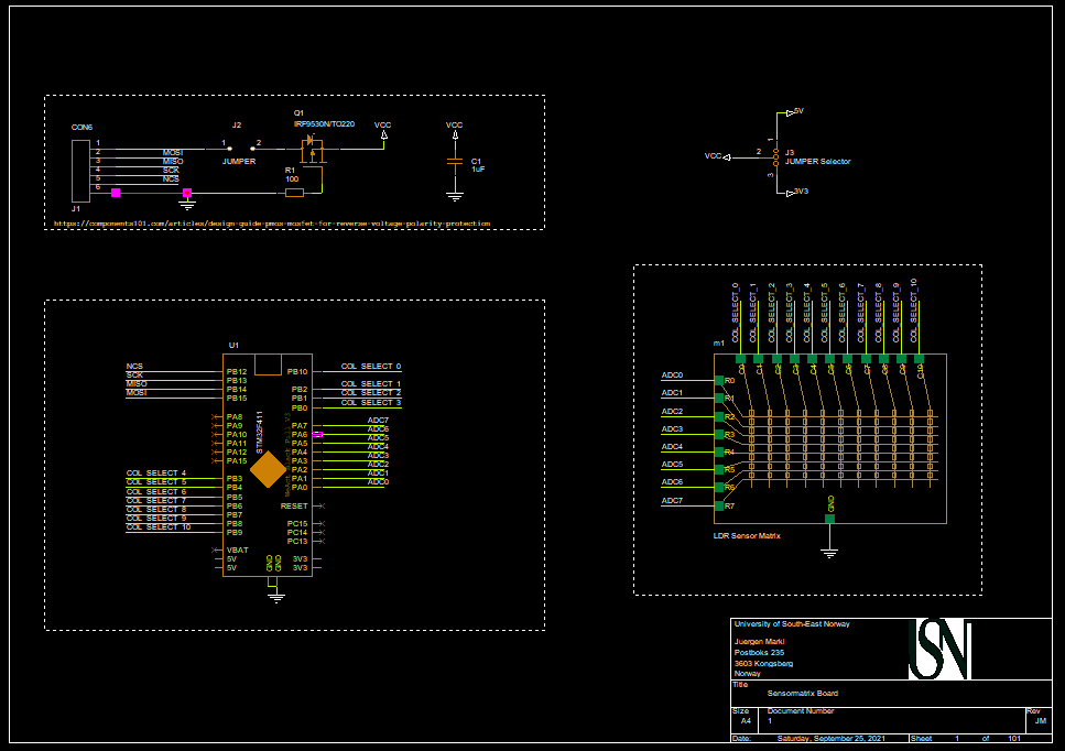
As the data also needs to be transferred form the µC on the matrix PCB to the central processing unit (CPU, does not require to be a computer processor, but also some kind of µC), as well as some pre-calculations on the raw data would be desired, the Arduino Nano is not sufficient with limited clock frequency. For this reason, and as i have access to two identical µC of the STM32F411 on a breakout-board, these were chosen. They also feature more functions for data throughput, namely a DMA (direct memory access), to transport data from memory to a periphery or vice versa. This will help with performance on transferring data from e.g. the ADC unit to memory or to a communication periphery.
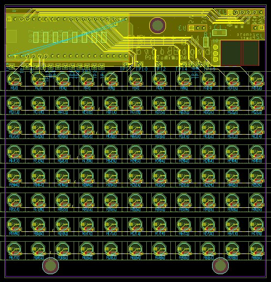
PCB Layout: The PCB mentioned above for the matrix will consist of 88 LDRs each and in total 2 shall be used as a first stage of tracking the ball. The prototype created during the last week performed as desired and thus the schematic for the final PCB was created using OrCAD Cadence, as it allows for complex hierarchical structures, which will be heavily used for this project, as many parts are just repeating circuits.
The most time consuming task of this was getting some structure into the PCB layout, as placing 88 LDRs with 88 diodes attached to them is not fun, so the place – replicate – function was used for this. Here you create one instance of the pattern, you want to repeat and store this as a module to reuse later. After placing all LDR and diodes somewhat aligned, the module was applied to them one row at a time to not have to figure out the positions of them in the matrix later (i tried this, was not fun).
Wiring up the matrix was pretty straight forward, the connection within one row was made on the backside, where the diode as SMD part was placed, the connection of the pins of the µC to the LDRs was done on the front side so no trace was crossed.
Connecting the rest of the nets was not problematic as space was plentiful, a reverse voltage protection in form of a P-Channel MOSFET was included, as this produces the lowest voltage drop on the input side (board designed to operate at 3.3V). This could result in a problem though, as the MOSFET available at the university, a IRF9520 & IRF9530 have a Gate-Source Threshold Voltage of -2 to -4V, so it is not certain if it will conduct with 3.3V. As an workaround for this, a jumper connector can be implemented to choose if the input voltage should be fed directly into 3.3V or trough the internal voltage regulator, which supports up to 5.25V input voltage. As the supply voltage is only needed for the µC, this should not affect the performance of the board in any way. With a 5V supply, the MOSFET should conduct and be able to supply up to 3A according to the datasheet.
For Interface with the CPU, SPI was chosen as it can be clocked at a few MHz for a reasonable short transmitting distance to achieve a high output rate.
Jostein
I am continuing the work to figure out the logic of the microprocessor that will be handling the input and output, as well as reading up on the electrical engineers recommended processor.
Theorycode for Smarter System
The idea is to digitalize the signal from the sensors (photresistors), setting up a certain threshold that registers the sensors as the on or off state and feed this data into a matrix.
The biggest problem with a photoresistor is that, as an analog unit, I am not certain if it isn’t always in an “on”-state as long as there is any level of light.
Each position in the grid would have to be carefully constructed within the program so that the machine always knows where each sensor is and how to run calculations off of this information.
By looping through the matrix at least each 1/40th of a second, and comparing the total value of the matrix it should be possible to catch and triangulate the direction of the ball from the data. The ball would be treated as if it was travelling across a triangle within a square with the first offset as its origin, as long as it was travelling downwards.
The flipper can fire on a random interval once it knows the ball is about to hit it.
We can program in some “lines”/correct delays where it knows that if the ball hit from this angle it will currently be within x-y on the flipper so to maximize points it should fire after a certain amount of time.
Theorycode for not so smart system
If sensor in array closest to flipper is triggered, fire flipper after random delay within test thresholds.
If the ball hits close to the edge then the flipper will fire immediately.
Petter
Did further research of what point system would work the best for our system. Started experimenting with connecting Arduino with a MySQL database through PHP to create two simple point system which added points to a MySQL database that’s displayed through the website leaderboards. One point system is simply just points being added to the database whenever the LDR sensor senses a difference in input. The other is points being added depending on time spent before the LDR sensor senses a difference.
Kristian
Started working on a system engineering style overview of the system, making direct connections to how our system will operate and relate to system requirements at many levels.
purpose of this work is to prevent last minute realizations that we need something we dont have, by going through everything we need for everything to work. Also cooperated with Jurgen on the pcb design, relating to physical constraints.
My workload this week was limited due to studying for 2 exams, 11th and 13th October.